Why do PCB boards need detection points?
Time:
2022-05-07 14:11
Source:
For those who learn electronics, it is a matter of course to set up test points on the circuit board, but for those who learn mechanics, what are the test points?
Maybe still a little confused. Thinking back to the first time I worked in a PCBA processing plant, I still remember that once, for this test point, I asked a lot of people and they all knew. It is mainly to test whether the components on the circuit board meet the specifications and solderability. For example, to check whether there is a problem with the resistance of a circuit board, the easiest way is to measure it with an electric meter. .
However, in a mass-produced factory, you can't use an electric meter to slowly measure every resistance, capacitance, inductance on each resistance sheet, even if the IC circuit is correct, so there is a method called ICT (In- Circuit-Test), which uses multiple probes (commonly referred to as "Bed-Of-Nails" fixtures) that simultaneously make contact with the wiring of all components on the instrument that need to be measured. Then, with program control as the main method and side-by-side as the auxiliary method, continuous measurement of these electronic components is carried out. Generally speaking, this test can be completed in 1-2 minutes for general boards, depending on the number of boards. The longer the component is used.
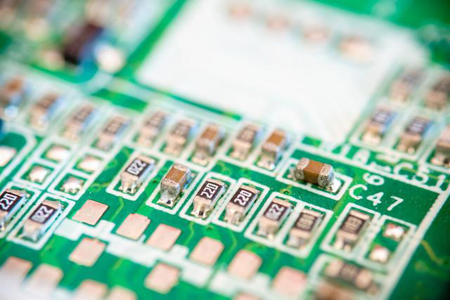
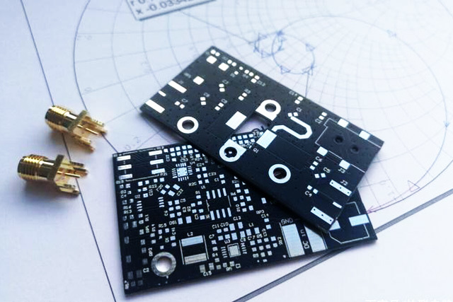
But if these probes are in direct contact with electronic components or solder pins, it is very likely to cause some electronic parts to be broken, so clever engineers invented a "test point", which is a pair of small dots attached to both ends of the part. , it does not require a solder mask (mask), it allows the test probe to touch these small points, without the need to directly touch the electronic components being measured.
In the early days, the circuit board was still a traditional plug-in type (DIP), and the soldering feet of the components were indeed used as test points. Since the soldering feet of conventional components are strong enough, they are not afraid of needle sticks, but misjudgment of poor probe contact often occurs. In other cases, since ordinary electronic components are subjected to wave soldering or SMT, there is generally a film of residual solder paste flux on the solder surface. This film has high impedance and often leads to poor probe contact. Therefore, at that time There are frequent test workers on the production line, who often blow with an air gun, or wipe the places that need to be tested with alcohol.
In fact, wave-soldered test points can also have probe contact issues. After the SMT was widely used, the test misjudgment situation has been greatly improved, and the application of test points has received great attention. Since the components of SMT are usually fragile and cannot withstand the direct contact pressure of the test probe, the direct contact between the probe and the parts and the welding feet can be avoided by using the detection point, which not only protects the components from damage, but also indirectly greatly improves the reliability of the test. sex, because there are fewer misjudgments.
However, with the advancement of technology, the size of the circuit board is getting smaller and smaller. It is already a little difficult to squeeze so many electronic components on a small circuit board. Therefore, in order to measure the problem of circuit board space , often pulling a small circuit board between the design side and the manufacturing side, which is a conundrum. The appearance of the detection point is generally round. Since the probe is also round, it is better to make, and it is easier to bring the adjacent probes closer, thereby increasing the needle density of the needle bed.
Using the needle bed for circuit testing has inherent limitations. For example, there is a limit to the minimum diameter of the probe, and needles with too small diameter are easily damaged.
There is also a certain limitation in the needle pitch, because each needle has to come out of a hole, and an extra flat cable needs to be soldered to the rear end of each needle. If the adjacent holes are too small, in addition to the problem of contact short circuit, the flat cable Cable interference is also a big problem.
Some tall parts cannot be implanted next to them. If it is too close to the part to be tested, the probe may be at risk of damage. In addition, due to the high part, it is usually necessary to make holes in the needle bed seat of the test fixture, which indirectly prevents the needle from being implanted. It is difficult to fit test points for all the components on the board.
Because these boards are getting smaller and smaller, the number of test points has been discussed again and again, and now there are some ways to reduce the test test, such as Nettest, TestJet, BoundaryScan, JTAG, etc.; there are others that hope to replace the original needle bed test. Methods, such as AOI, X-Ray, but now it seems that each kind of experiment can not replace ICT 100%.
In terms of ICT's ability to implant needles, the manufacturer of supporting equipment should be consulted, that is, the minimum diameter of the detection point, and the shortest distance between adjacent detection points, generally have a minimum value between the hope and the minimum ability to achieve, while large factories The chamber of commerce requires that the distance between the minimum test point and the minimum test point should not exceed how many points, otherwise the fixture will be easily damaged.
Relevant news


